Advanced Semiconductor Materials

High-quality materials for research and industrial applications

Our Products

These prices serve as reference only. Please note that the prices listed here do not include shipping and transaction fees. Typical sizes for most synthetic crystals listed below are 6-10 mm on sides and <0.1 mm to 0.4 mm thick. All crystals come with technical data sheets. We supply: bulk single crystals (boules, ingots), crystalline plates (wafers) of various diameters, crystalline rods, monocrystalline powders. HS code for customs procedures: we typically use 3818.00.100 which corresponds to doped silicon. For more information about crystal properties or additional details, please contact us at info@crystalab.org

Materials

Our company specializes in growing high-quality single crystals from high-purity metals and their compounds. Our main production materials include:

Bismuth (Bi) and its compounds

Bismuth telluride (Bi2Te3), Bismuth selenide (Bi2Se3), Bismuth sulfide (Bi2S3)

Molybdenum (Mo) and Tungsten (W)

Molybdenum disulfide (MoS2), Tungsten disulfide (WS2), Tungsten diselenide (WSe2)

Tellurium (Te) and its compounds

Lead telluride (PbTe), Cadmium telluride (CdTe), Tin telluride (SnTe), Antimony telluride (Sb2Te3)

Doping elements

For precise control of crystal properties we use: Sulfur (S), Selenium (Se), Iodine (I). These elements allow regulation of: conductivity type (n- or p-type), band gap, thermoelectric characteristics.

We also select materials and growth technology according to customer's specific needs.

Email us at info@crystalab.org to discuss your project parameters!

About CrystaL Laboratory

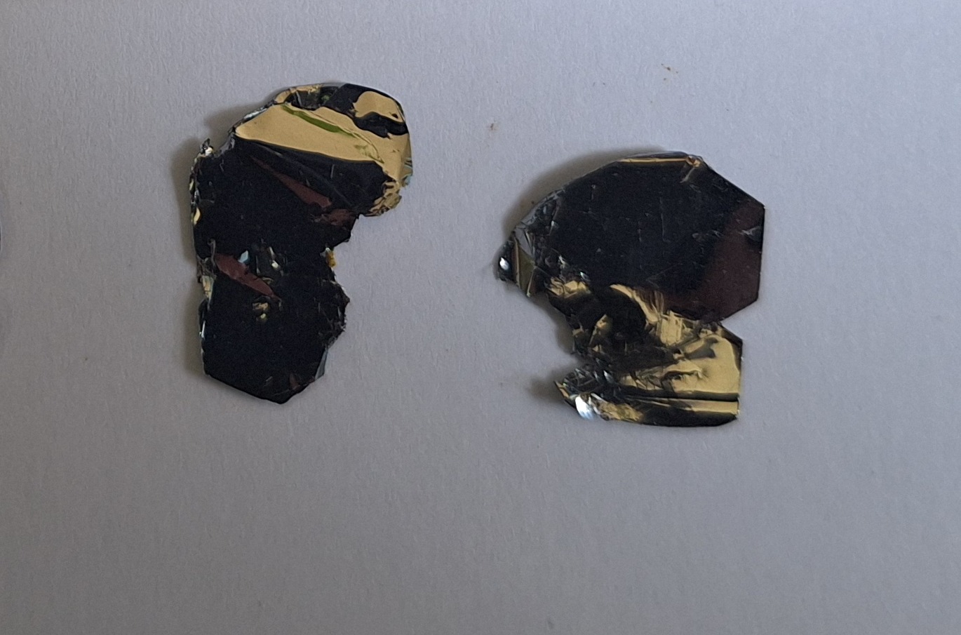
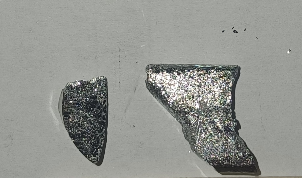
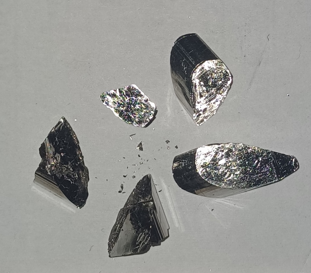
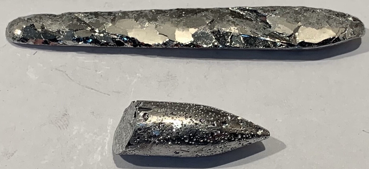
Our company is a manufacturer of high-quality single crystals. Specializing in advanced crystal growth technologies, we supply products for high-tech industries, scientific research and innovative developments.

We provide the market with high-quality monocrystalline materials with precisely controlled properties, contributing to the development of thermoelectric, optoelectronic and semiconductor technologies.

Key advantages:

In-house production

full cycle from raw material purification to monocrystal growth

Use of 5N-6N purity materials

(99.999% - 99.9999%)

Modern technologies:

Bridgman-Stockbarger method (vertical and horizontal growth), zone melting, zone sublimation growth, vapor transport growth

Our clients and partners:

We cooperate with manufacturers of thermoelectric devices, semiconductor electronics companies, research institutes, new materials development centers.

Why choose us?

High repeatability of crystal parameters from batch to batch, as well as optimal price/quality ratio.

High Quality

Strict quality control at all production stages and precise compliance with specified parameters

Global Shipping

Worldwide delivery in compliance with all requirements using international logistics companies

Technical Support

Expert assistance in development and production of monocrystals according to your technical requirements

Contact Us

Contact Information

Chisinau, Republic of Moldova

+373 78220926

info@crystalab.org